Picture of the Month: Atom by atom towards the perfect LED From the Institute of Applied Physics
Not all electron microscopes are the same. Since the first set-up in 1931, researchers have been working at great expense to achieve ever higher resolutions. The most powerful electron microscope at the TU Braunschweig, the TEM, is therefore completely sealed off from mechanical vibrations (such as trams rattling past) and magnetic fields (such as the earth’s magnetic field) at the LENA research centre.
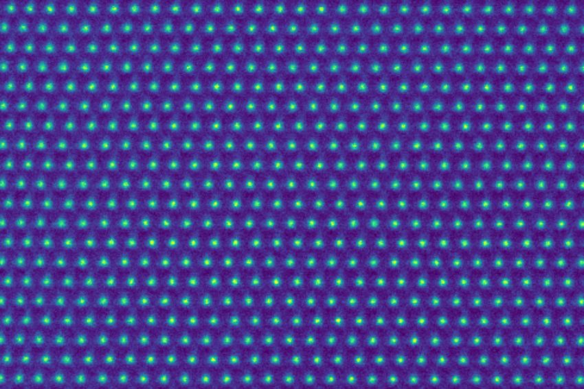
The TEM allows a look at the atomic structure of the semiconductor gallium nitride (GaN). Picture credits: Daesung Park/TU Braunschweig
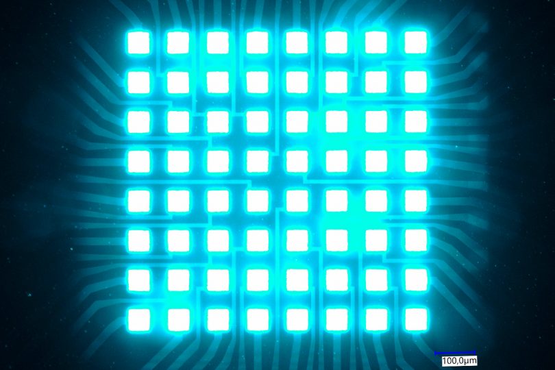
Our picture of the month gives an insight into what the super device is capable of: the atomic structure of the semiconductor gallium nitride is finely lined up. As part of the QuantumFrontiers cluster of excellence and Quantum Valley Lower Saxony, researchers from TU Braunschweig and the Physikalisch-Technische Bundesanstalt are jointly developing tiny blue LEDs from the material gallium nitride. During the complex LED production in the clean rooms of the Institute of Semiconductor Technology, gallium nitride is repeatedly fabricated, coated and etched. The researchers find out how good the next LED generation has become primarily through electron microscopy. The high-resolution TEM makes it possible for the scientists to go into detail, atom by atom, even with material samples that are already nanometres in size.
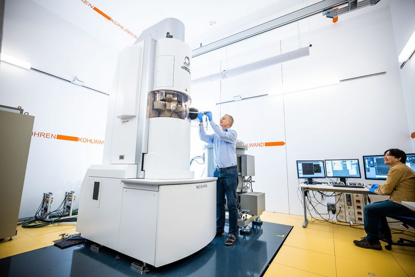
Dr Heiko Bremers and Dr Daesung Park (from left) at the TEM in the LENA research centre. Picture credits: Jan Hosan/TU Braunschweig