International and interdisciplinary: A team for luminous nanosensors Focus on Research: At the Limit of Measurability
An inverview with Dr. Hutomo Suryo Wasisto, head of the junior research group OptoSense (Optochemical Integrated Nanosystems for Sensing) at the Laboratory for Emerging Nanometrology (LENA), and his doctoral candidates Tony Granz, Gregor Scholz and Klaas Strempel, about cultural diversity in science, the appeal of gallium nitride and why young scientists especially should venture out of the lab every now and again.
Dr. Wasisto, you are from Indonesia, earned your bachelor’s degree there and your master’s degree in Taiwan. How did you come to join this team here in Braunschweig?
In a rather roundabout way (laughs). I always had this dream of doing research in Europe. Germany was my first choice, mainly because it is very strong in technology. In Taiwan, I researched silicon technologies with the aid of an industry grant, and was able to earn my doctorate here in Braunschweig at the Institute of Seminconductor Technology under Professors Erwin Peiner and Andreas Waag. Right after that, I received a job offer from Georgia Tech (Georgia Institute of Technology) in Atlanta. So I basically dropped everything here and went to the US, but only for a little under a year. When I was given the chance to head this junior research group, I was delighted to come back to Braunschweig.
Your team is made up of physicists, electrical engineers and chemists. Doesn’t this lead to “cultural” problems?
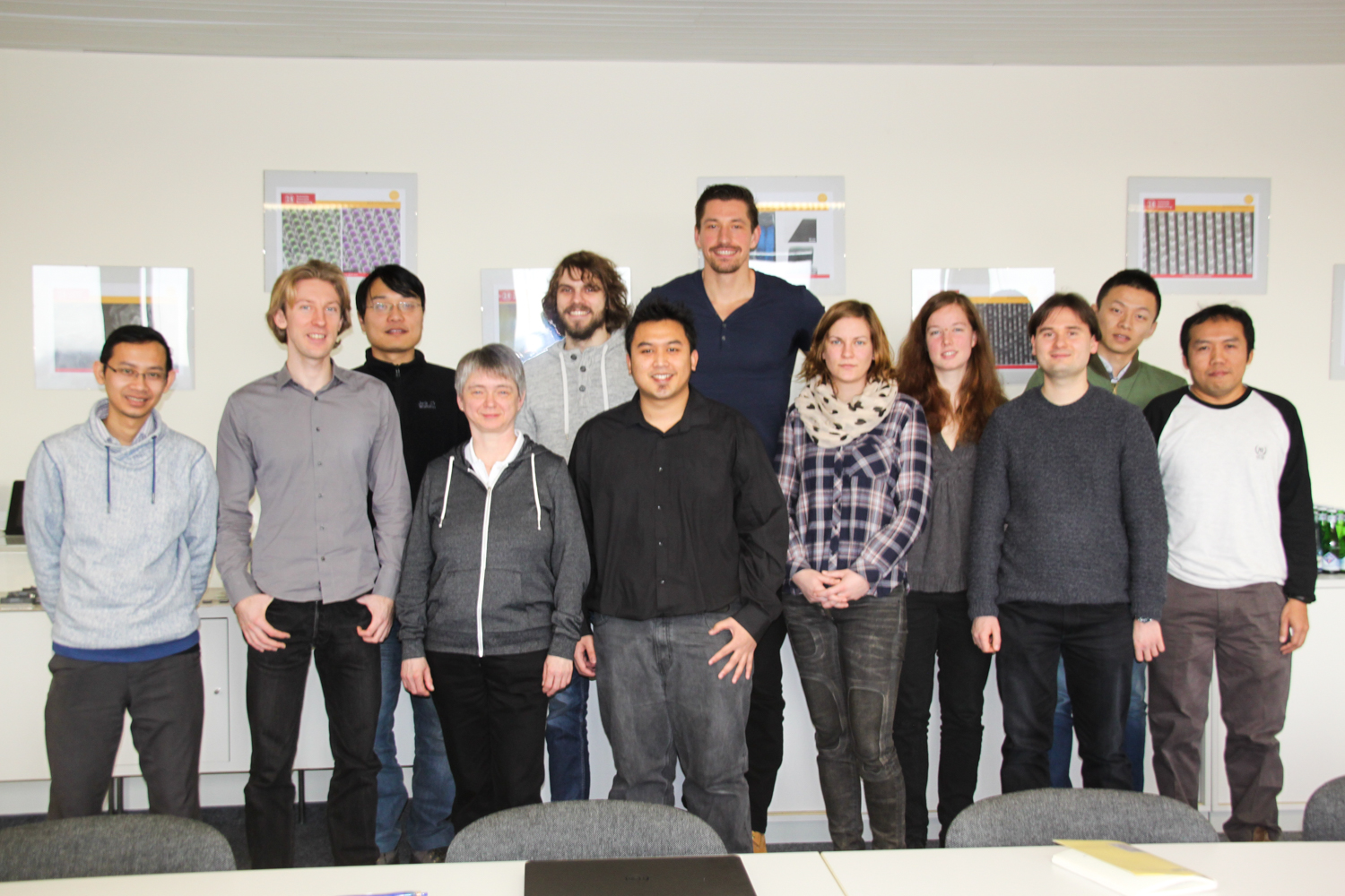
Left to right: Nursidik Yulianto, Nicolai Markiewicz, Feng Yu, Angelika Schmidt, Klaas Strempel, Dr. Hutomo Suryo Wasisto, Tony Granz, Juliane Breitfelder, Heidi Boht, Gregor Scholz, Wenze Wu, Iqbal Syamsu. Credit: Andrea Hoferichter: TU Braunschweig
Wasisto: Well, of course engineers and physicists have completely different work methods. Physicists want to understand the basics first, and then ask themselves which approach is the most promising. Engineers start by assembling something and then look to see if it works afterwards. But they also use knowledge taken from basic physics research and run simulations in order to make predictions. So we are learning a lot from each other.
Scholz: Besides, we are already used to each other (grins). Here at TU Braunschweig, electronic engineering and physics belong to the same department. During our master’s degree programme, many of us chose Nanosystems Engineering (NSE) as a specialisation. This incorporates electrical engineering, physics, chemistry and biology. It’s all about working across intersecting disciplines.
Wasisto: And our research is very application-oriented. We have many government-funded projects with partners from industry.
Strempel: That’s why I joined this working group: I wanted to do application-oriented work even though, as a physicist, I am mostly focussed on getting to the bottom of mechanisms and understanding them.
Granz: As a scientific engineer, I see myself at the crossroads between fundamental research and economic applications. Every day, we try to turn our natural scientists’ complex findings into practical applications for society. To do that, we have to work very closely together.
You are working with gallium nitride. Most people are probably unfamiliar with that material. What is so attractive about it?
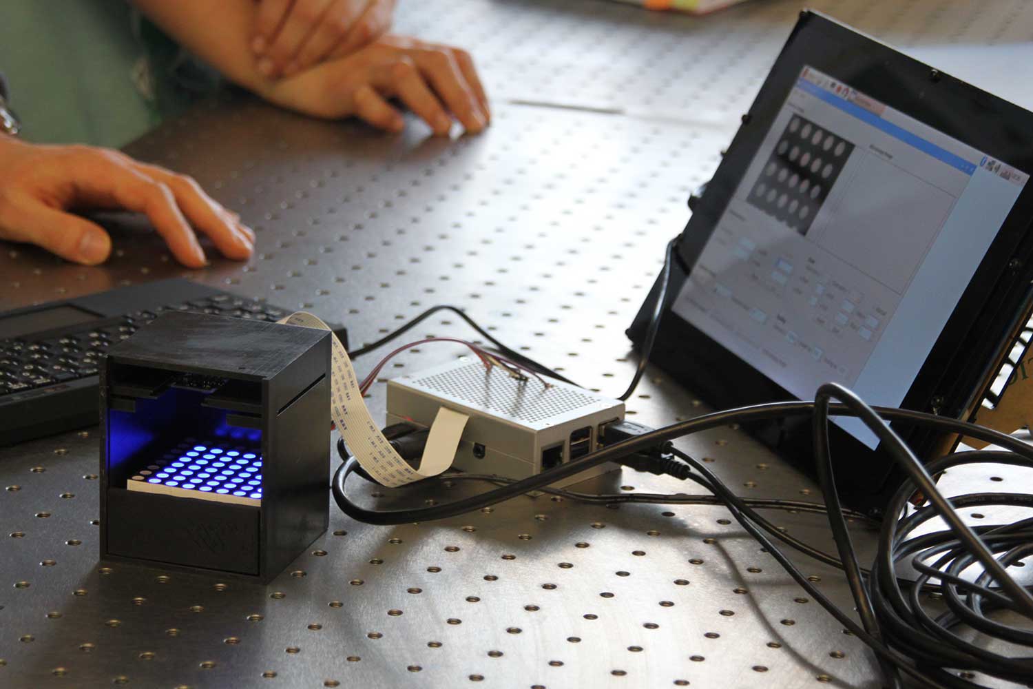
The blue LEDs can be controlled individually using the tablet, or dynamic light patterns can be produced. Credit: Andrea Hoferichter/TU Braunschweig
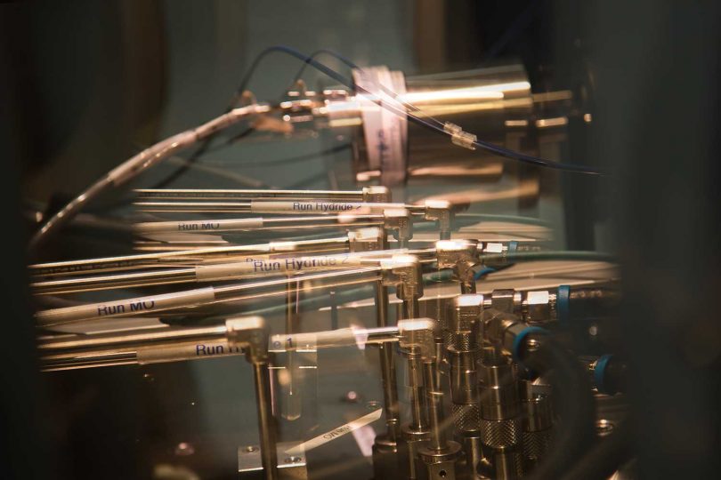
Wasisto: You could say the semiconductor gallium nitride is the new silicon. By now, we have a very good understanding of silicon and have more or less fully exploited it from a scientific point of view. With gallium nitride, whole new avenues are opening up. For example, it could make electronic components even more powerful. In our working group OptoSense, we plan to develop new platforms for sensors using this material, which may in the future be used in biomedicine and to measure pollutants. We are working on the electronics, optical components, energy recovery and energy supply. And we don’t want to measure any which way, but rather selectively and very accurately. That is why we are cooperating closely with the German National Metrology Institute (PTB).
Strempel: At this point, researchers all over the world are working with gallium nitride. The community is already quite vast. The boom began in the 1990s, when the first blue light-emitting diode (LED) was made from the material. In 2014, the Nobel Prize for physics was awarded for this.
Scholz: Exactly. Before that, there were only the red and green LEDs that we remember from the electronic assembly kits we had as kids. It was only with the advent of blue LEDs made of gallium nitride that we were able to mix white light. This was a major breakthrough. Since then, there have been countless new applications in lighting technologies and consumer electronics, but also in science, for example in lasers.
Granz: But we want to take it a step further, because gallium nitride also has excellent electrical properties. As an example, all the electronics (such as transistors) surrounding a sensor could be made of gallium nitride instead of silicon. Zinc oxide, which is currently the most widely-used sensor material, could be replaced by gallium nitride. It is therefore conceivable that entire sensor systems could be made solely of gallium nitride, which would be a tremendous help in further miniaturisation.
What role does your group play in the gallium nitride community?
Wasisto: We are one of leading groups worldwide. Especially because we do not use the semiconductor two-dimensionally, but rather three-dimensionally, for example as nano wires or nano fins. This opens up entirely new possibilities. The only direct competitor in the field of 3D gallium nitride high-performance electronics is a team at MIT, the Massachusetts Institute of Technology, in the US. Whenever we are at a conference, like we were a few months back in Orlando and San Francisco, and MIT researchers give presentations, we always ask them a lot of critical questions (laughs). And vice versa, of course.
How important are these international conferences?
Wasisto: They are very important, especially if you want your research to be visible on an international level.
Granz: Conferences are also important for finding out if the topic you are working on is even still relevant and of interest to the industry.
Wasisto: Exactly. Just researching away, alone in your lab, is pointless. Nobody would know what we’re doing. That’s why publishing your work in renowned scientific journals is also very important. I once received a call from the industry about one of our projects. They were interested in patenting a technology. Without conferences and publications on the technology, that would never have happened.
Granz: However, scientific writing is a skill that needs to be learned. In the beginning, you send a draft to your advisors, co-authors and reviewers, and when you get the text back, it is covered with red, full of corrections, questions and suggestions for improvement. You gradually get a feel for it, and it becomes much easier.
Wasisto: That’s perfectly normal; it was the same for me at the start. You just have to keep working on it. It’s also very good preparation for your doctoral thesis. That’s when you really have to deal with such questions. And by then, you will have gained enough experience that you can answer them quite readily. I personally was actually quite relaxed during my thesis for just that reason.
How international is the OptoSense team?
Granz: At our last Christmas party, they showed a diagram where you could see that our group comprises roughly as many German scientists as scientists from Indonesia, Russia, Spain and China. We have become more and more international in recent years. That’s definitely good preparation for the global workplace. We are learning how people from other parts of the world do scientific work, and what we need to pay attention to on a social level.
Wasisto: For me, the connection to Indonesia is obviously very important. Many researchers like myself go to other countries to earn a doctorate or to work. Yet it would be preferable to keep well-educated engineers and scientists in the country. That’s why I initiated IG Nano, the Indonesian-German Centre for Nano and Quantum Technology. We support the scientists there and, with their help, advance our research here. It’s a true win-win situation.
Text: Andrea Hoferichter