Picture of the Month: Etched Topographic Map in Gallium Nitride Submitted by the Institute of Semiconductor Technology
From red to yellow to blue: for 40 hours, doctoral student Klaas Strempel from the Institute of Semiconductor Technology etched a gallium nitride semiconductor crystal with hot potash lye. He uses it to investigate how the etching speed of the lye depends on the symmetrical crystal structure. Starting from the yellow plateau, three micrometer deep canyons now extend into the semiconductor – the bluer, the deeper. What looks like sunlight, on the other hand, are the up to one micrometre thin webs of gallium nitride, or what is left of it after the long etching process. Such so-called fins are further processed at the institute into microscopic transistors.
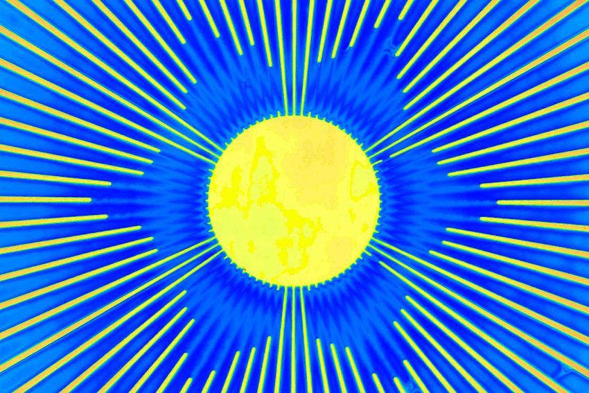
The potash lye makes the symmetrical crystal structure of gallium nitride visible. Picture credits: Klaas Strempel/TU Braunschweig
Gallium nitride fins are regarded as the key to a new generation of transistors in microelectronics. In comparison to the predominantly used silicon, gallium nitride can process higher frequencies at high power. The quality of the etched surfaces is particularly important. Therefore, scientists at the Institute of Semiconductor Technology are trying to better understand the etching process.
The symmetrical pattern of the image results from the regular hexagonal crystal structure of gallium nitride. Depending on the crystal direction, the potash solution eats through the fins of the semiconductor structures at only 1 to 100 atomic lengths per hour. In the process, the webs are dissolved ever thinner or even altogether. Where the rays are uninterrupted, the crystal structure is most inaccessible to the lye. The symmetry shows how this crystal structure is repeated every 60 degrees.
Pixel by pixel towards the topographic map
The image is basically the topographic map of an etched semiconductor crystal, taken with a laser scanning microscope. Unlike other optical microscopes, the laser scanner works confocally. This means that it does not illuminate the whole specimen at once, but scans the object pixel by pixel and focal plane by focal plane. Knowing how much light is reflected by each pixel at all focal planes allows the construction of a three-dimensional image with height information, accurate to about 10 nanometres. By way of comparison, the smallest bacteria are 30 times larger, but to peek out of one of the trenches, they would have to be stacked at least ten high.