Recipe for tiny 3D light-emitting diodes Focus on Research: At the Limit of Measurability
Like she does most mornings, Jana Hartmann exchanges her street shoes for white clogs, puts on white overalls and latex gloves and dons a medical cap. Then she enters “her realm”: the clean room at the Institute for Semiconductor Technology, on the 10th floor of the TU tower block on Hans-Sommer-Straße. Any kind of dirt is taboo here, hence the protective clothing. Then the electronic engineer resumes work on her doctorate.
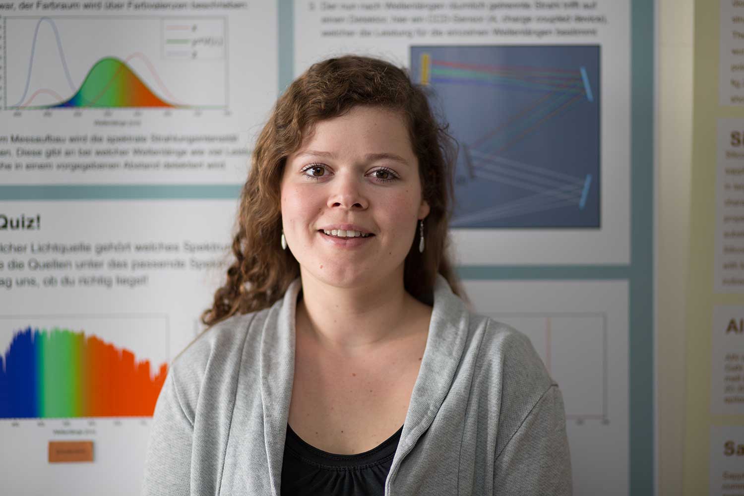
Jana Hartmann, Research Fellow at the Institute of Semiconductor Technology of the TU Braunschweig. Credit: Jonas Vogel/TU Braunschweig
Inside the clean room is a machine – taller than a man, several metres long and made of gleaming stainless steel – for metalorganic vapour-phase epitaxy, also lovingly called “MOVPE”. “I have just finished writing a new recipe. I want to start this quickly, so that it will be done by tonight”, the researcher says. No need to add that this is not about the invention of a cool new chocolate cake or other culinary delight. During MOVPE, Hartmann combines various gases to create tiny three-dimensional light-emitting diodes – 3D LEDs for short. They are tiny walls of gallium nitride, thinner than a single human hair.
Recipe for light-emitting diodes
“3D LEDs have an extra-large surface and are thus able to emit more light”, she explains. In the future, they may become much more efficient than conventional, planar LEDs, and might be used in highly-sensitive sensors, and in lighting and laser technologies.
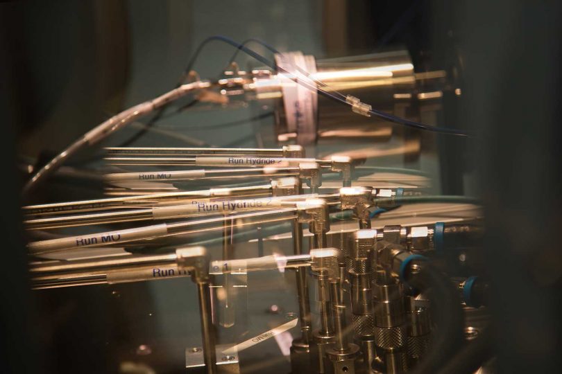
Hartmann displays her recipe on the MOVPE unit’s screen. It sets out which ingredients will be added, when and at what temperature or pressure. Ammonia is used, along with chemical compounds containing either gallium, indium or silicon. At the heart of the machine is a stainless-steel reactor the size of a coffee maker. It is located in the glovebox, a glass-fronted box from which arm-length rubber gloves protrude. “The glovebox contains pure nitrogen, to keep oxygen and other substances in the air from disrupting the deposition process”, the researcher explains.
She slips her hands into the gloves, reaches inside the glovebox and opens the reactor’s lid. A rotary disk similar to the ones found in microwaves becomes visible. It can hold wafers with two inch in diameter, called templates, and can be heated to over 1,000°C. Once the lid is closed, the reaction gases flow from the reactor lid onto the templates – like from a shower head – and react chemically to form a gallium nitride crystal.
An in-house product
The templates themselves are also produced here at the Institute for Semiconductor Technology. They consist of a transparent sapphire wafer with a gallium nitride layer, plus a silicon oxide layer with holes or razor-thin slits above that. The LEDs grow in these slits like walls or “fins”, as they are called here at the institute. “I have been researching fin LEDs made of gallium nitride for two years now”, says Hartmann. Before that, she mainly used to deposit tiny columns. Fins, however, are much stronger and have an even larger surface relative to the wafer’s dimensions. “The reason for this is mainly that 3D LEDs cannot be placed as close to one another as we would like”, she explains.
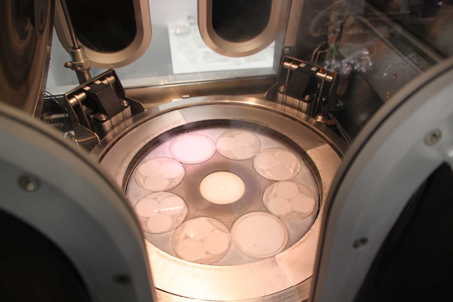
These wafers are coated with epitaxy to build up three-dimensional LED structures. Credit: Andrea Hoferichter/TU Braunschweig
During MOVPE, the fin LEDs first grow in height and then in width. Around the gallium nitride core, a shell is deposited that contains, among other things, indium gallium nitride. The quantity of indium determines the wavelength and thus the colour of the LED’s light.
To get started, Hartmann places new templates onto the reactor’s rotary disk, closes the lid, once more checks the settings on the machine’s monitor, and then presses “Run”. The process begins. It will take a good 6 hours to complete. In the meantime, the researcher examines older samples under the scanning electron microscope and makes them emit light by means of a process called cathodoluminescence. “This allows me to see the 3D LEDs’ properties quite well: for example, how high and wide they ended up being and how much indium they contain”, she says.
A 3D microscope for diabetes research
A few months from now, Jana Hartmann will write up the results of her experiments in her doctoral thesis. And after that? “Then I can fully dedicate my time to leading a junior research group within the QUANOMET research alliance”, she comments. The group works on diabetes research in the broadest sense of the term. The team plans to develop a small, inexpensive microscope made from tiny LEDs to support research into insulin-producing pancreatic islets. “Not only are we trying to image the cells optically, we also want to measure processes within the cells, such as how much oxygen they use”, says Hartmann.
Her visits to the clean room laboratory will then become very infrequent. “I guess I will mainly be dealing with organisational tasks. But that’s fine: I like organising”, laughs the engineer. There is only one thing that makes her a little sad: saying goodbye to MOVPE. “For four years now, I have been working with this machine on almost a daily basis. I think I will miss it quite a bit.”
Text: Andrea Hoferichter