Microchips replacing microscopes: How Superlight Photonics plans to make it big with tiny LEDs Focus on Research: At the Limit of Measurability
In terms of location, the start-up project Superlight Photonics is already at the top: its office is on the 14th (and top) floor of the TU tower block on Hans-Sommer-Straße. From here, the six researchers plan to take over the nano world, not only scientifically but also commercially speaking. “We are developing microchips that will be able to show structures at a scale of a millionth of a millimetre, and even single molecules”, says team leader Sönke Fündling. The centrepiece of their technology: nanometre-sized blue light-emitting diodes (LEDs) made of gallium nitride.
Fitted with such tiny LEDs, the Superlight chips will be able to compete with many labour-intensive and time-consuming analyses at specialised laboratories, as they offer fast and easy-to-interpret measurement results. “Among other possibilities, they can be used in the medical field: for example, for rapid blood testing or as implants to control insulin”, says Fündling. They are also suitable as detectors of air- and waterborne pollutants. The possibilities for application are manifold. “The direction our research takes will mainly depend on the type of investor that we can attract”, says the physicist.
Like a shadow image of blood cells

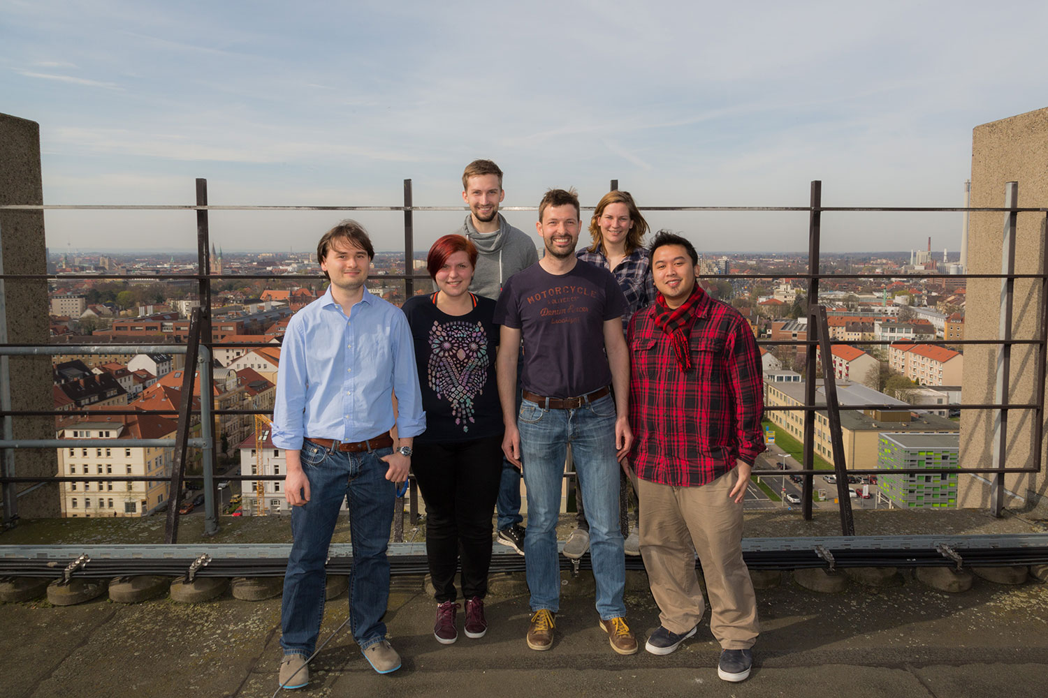
From left to right: Gregor Scholz, Daria Bezshlyakh, Frederik Steib, Dr.-Ing. Sönke Fündling, Juliane Breitfelder, Dr.-Ing. Hutomo S. Wasisto. Credit: Jonas Vogel/TU Braunschweig
The innovative microchips’ working principle compares to a light microscope, except that the light emerges from individually controlled nanoLEDs instead of a white light lamp. A photodetector functions as the human eye, registering where light shines through the sample, and where not. “When we record such a shadow image – for example of blood cells – from various angles, we can generate a very precise image”, Fündling explains. The smaller the nanoLEDs, the greater the resolution. The LEDs can even make individual molecules visible, if they have been marked beforehand with a fluorescent substance.
“The biggest challenge for our project is the material”, says Fündling. Gallium nitride is very hard, and difficult to process. Determining the ideal conditions for processing gallium nitride is something that researchers are currently working on a few floors below Superlight Photonics, at TU Braunschweig’s Institute of Semiconductor Technology. This institute is a sort of scientific home for Fündling and his colleagues, and its director, Professor Andreas Waag, is their start-up’s mentor.
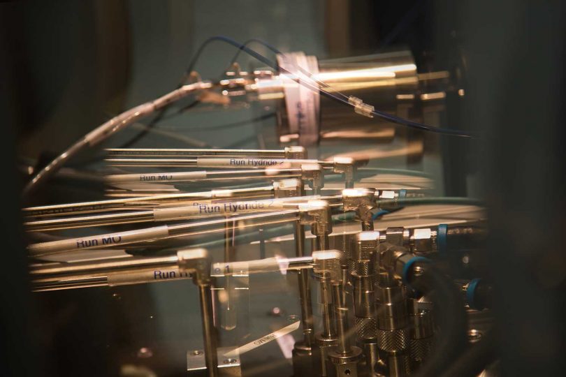
In a tall stainless steel machine, they evaporate gallium nitride in layers onto silicon or sapphire wafers to obtain large LEDs. With the use of electrically charged particles, they scribe razor-thin rifts into the material and etch away the debris with chemicals. What is left is a kind of checkerboard pattern of tiny LEDs. The scientists then use scanning electron microscopes and other procedures to check how well these LED patterns have turned out.
Investors wanted
“We are pursuing a second processing approach, in which a larger gallium nitride LED is contacted by a nano-structured silicon microchip”, says Fündling. That chip is currently manufactured by an external partner. Another important task on which the researchers are working is the development of the control software for both microchip architectures, as well as a functional, attractive casing.
By the end of the year, the team will present a prototype to demonstrate the microchips working principle. They will then need investors to take it to the next level. “It’s quite an ambitious schedule. We won’t have any chance to get bored in the very next future for sure”, Fündling jests. However, it is a good thing there are relaxing moments too, like when the sun sets over Braunschweig – quite a treat to watch from the tower’s 14th floor.
Text: Andrea Hoferichter

