Picture of the Month: False colours in the UV-LED From the Institute of Semiconductor Technology
UV light has a wide range of applications: Depending on the wavelength and energy intensity of the light, UV LEDs can sterilise surfaces and water, make tomatoes grow particularly tasty or be used in dermatology for skin treatments. However, the efficiency of the “invisible” UV LEDs can still be improved. A team at the Institute of Semiconductor Technology is researching this. Their approach: The crystal layers within the UV LEDs are laid out three-dimensionally as a microstructure instead of as a two-dimensional disc, as was previously the case. Analyses under the electron microscope – as seen here in the Picture of the Month June – indicate a high efficiency of the UV LEDs constructed in this way.
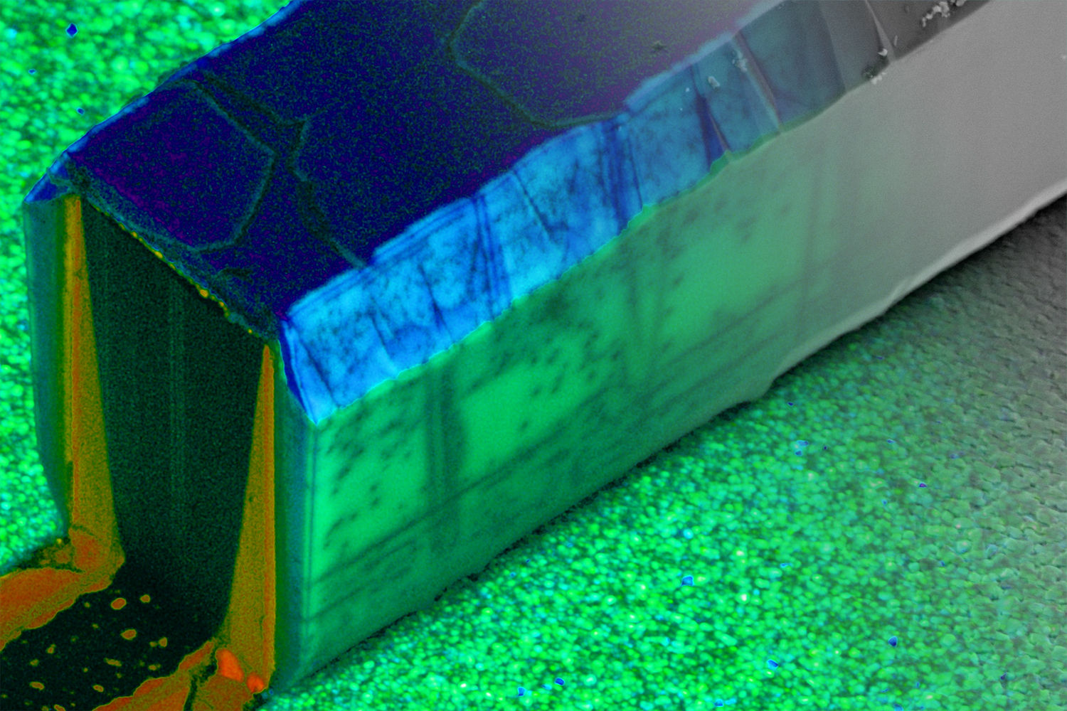
Picture credit: Hendrik Spende, Christoph Margenfeld/ TU Braunschweig
UV light is not perceptible to the human eye. However, with the help of a cathodoluminescence setup on a scanning electron microscope, this light emission can be made visible with spatial resolution. The electron beam, which is normally used to image the surface, also stimulates the electronic structure of the semiconductor material in the LED. This subsequently emits in light of different wavelengths, whereby the wavelength depends on the exact elemental composition or crystal structure. In this case, the wavelength of the light is translated into false colours with the help of a scale and leads to the colourful appearance of the Picture of the Month. The small diameter of the electron beam makes it possible to achieve a resolution of well below 100 nanometres, i.e. below the optical diffraction limit.
Black spots indicate crystal defects
These false colours can be used to determine at which points the crystal emits light of which wavelength. The intensity of the emission is reflected in the brightness of the image. Dark spots mean less emission and indicate defects in the crystal structure. The higher the density of black spots, the lower the quality of the crystal. This has a direct influence on the efficiency of the UV LED.
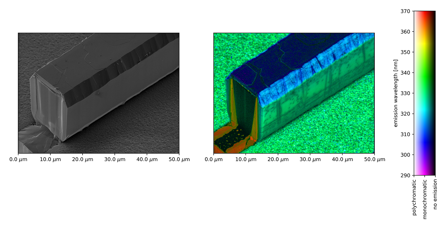
Basics for the Picture of the Month: The electron microscope depicts the topography of the aluminium gallium nitride crystal in greyscale (left). Wavelength and intensity of the light emitted under electron irradiation are translated into false colours with the help of a colour scale (right). The result is the Picture of the Month June. Picture credits: Hendrik Spende/ Christoph Margenfeld/ TU Braunschweig.
The team at the Institute of Semiconductor Technology would like to reduce the number of defects within the gallium nitride crystals and is therefore researching an alternative component geometry. Usually, the crystals are built up layer by layer on a wafer, a crystalline disc about five to ten centimetres in size. To do this, the wafer is loaded onto a hot substrate at 800 to 1,200 degrees Celsius in a reactor, and gases containing aluminium, gallium and nitrogen flow over it. These react on the hot substrate and the aluminium gallium nitride crystal is formed on the wafer.
Cross-section of a fin
At the Institute of Semiconductor Technology, this process has now been adapted so that the three-dimensional structures, also called fins, form first. The wafer surface is masked with silicon dioxide and the growth conditions in the reactor are adjusted so that gallium nitride fins grow upwards in the non-masked areas (dark V-shaped and orange area in the picture). In a further step, the light-emitting envelope of aluminium gallium nitride is grown around this core (green, turquoise and blue areas of the fin). The cross-section of such a fin can be seen in the Picture of the Month.
The defect density, i.e. the number of spots that do not emit light, is 100 to 1,000 times lower on the sidewalls of the novel structures than in aluminium gallium nitride crystals, which are produced two-dimensionally as before. The team at the Institute of Semiconductor Technology hopes this will increase the efficiency of UV LEDs, which will help close the efficiency gap between UV and conventional LEDs. While conventional LEDs have energy efficiencies of 80 percent, UV LEDs currently have efficiencies of one to two percent. In the future, this basic research could contribute to using UV LEDs even more frequently in plant cultivation, in dermatology or for disinfection, or enable applications of LEDs in the field of quantum computing. It is integrated into the Quantum Frontiers Cluster of Excellence and the EU project Smile, and emerged from the BMBF-funded project “3D-UV-LED”.