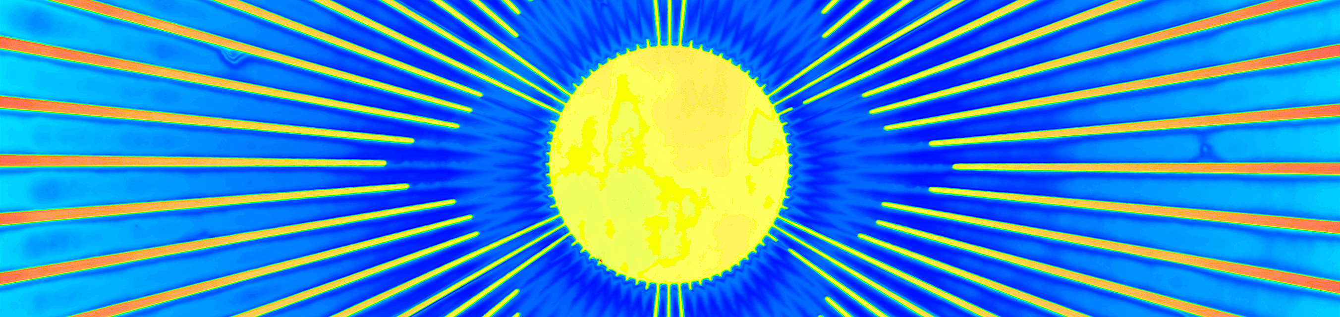
Topographic map of an etched semiconductor crystal, taken with a laser scanning microscope in the Institute of Semiconductor Technology. Picture credits: Klaas Strempel/TU Braunschweig
This image is part of: Picture of the month. Please note the copyright of this image.